

Semiconductor Bonding Market Expected to Grow at 4.35% CAGR and Reach USD 1.86 Billion
Semiconductor Bonding Market
Semiconductor Bonding Market Size, Share and Research Report By on Process Type Type (Die-To-Die Bonding, Die-To-Wafer Bonding, and Wafer-To-Wafer Bonding)
Semiconductor Bonding Market: Advancements in chip packaging, 3D integration, and high-performance electronics are propelling growth in the semiconductor bonding market.”
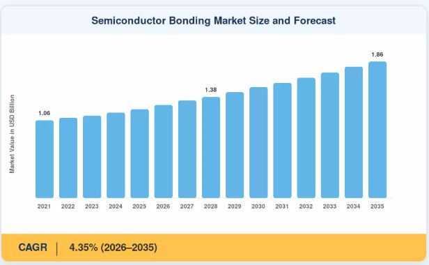
TAIPEI, TAIPEI, TAIWAN, August 7, 2026 /EINPresswire.com/ -- The Global Semiconductor Bonding market was valued at USD 1.21 billion in 2025 and is projected to grow from USD 1.27 billion in 2026 to USD 1.86 billion by 2035, registering a CAGR of 4.35% during the forecast period 2026–2035. Government semiconductor subsidies exceeding USD 85 billion collectively across the United States, European Union, South Korea, and Japan are channeling investment toward bonding capacity rather than traditional lithography-led fab expansion. — Market Research Future (MRFR)
This policy-driven capital reallocation is anchoring the market in a multi-year growth cycle independent of front-end node transitions. The market's 4.35% CAGR reflects the convergence of government semiconductor subsidies (+0.90% impact), HBM and 3D NAND layer scaling (+0.75%), automotive electrification and ADAS (+0.55%), and chiplet standardization (+0.50%) accelerating across the world's largest OSAT and memory-fabrication economies simultaneously.
A generational transition is underway as monolithic system-on-chip designs surrender ground to disaggregated architectures that rely on die-to-die and wafer-level bonding. Legacy wire-bonding lines that once dominated back-end assembly are rapidly being augmented and in high-performance segments replaced by thermocompression, hybrid, and fusion bonding systems.
Equipment suppliers combining plasma activation, inline alignment metrology, and bonding in a single cluster tool have demonstrated cycle time reductions of around 40%, leading to tool utilization in excess of 70% and speeding the return on investment for outsourced assembly and test providers. Asia-Pacific is anticipated to hold a revenue share of 44.5%, supported by concentrated OSAT capacity in Taiwan, South Korea, and China. North America accounts for the second-largest market at around 28%, pushed by CHIPS Act payments, while Europe is growing its packaging footprint through the EU Chips Act. Asia-Pacific is expected to enjoy the market's strongest regional growth at a projected 5.28% CAGR through 2035.
Get Full PDF Sample Copy of Report: (Including Full TOC, List of Tables & Figures, Chart) @
https://www.marketresearchfuture.com/sample_request/10738
➤ How Significant Is the Semiconductor Bonding Market's Growth?
The semiconductor bonding market's trajectory from USD 1.21 billion in 2025 to a projected USD 1.86 billion by 2035 represents a steady, policy-anchored expansion over the forecast decade, reflecting the structural shift from wire-bonding-dominated back-end assembly toward thermocompression, hybrid, and fusion bonding platforms that underpin disaggregated chip architectures. The market's 4.35% CAGR is anchored in a packaging-investment supercycle where government subsidy programs, high-bandwidth-memory scaling, and automotive electrification are all converging to make bonding equipment a strategic rather than commoditized category within the broader semiconductor equipment supply chain.
Die bonder equipment captured an estimated 39.5% share of the market in 2025, reflecting its entrenched role in high-volume consumer and memory assembly, while hybrid bonder equipment is projected to advance at a 4.60% CAGR through 2035, driven by demand from logic and high-bandwidth memory integration.
By interconnect level, die-to-die bonding accounted for roughly 57.5% of the market in 2025, underscoring the shift toward disaggregated chip architectures, while wafer-to-wafer bonding is on course for a 4.85% CAGR to 2035, accelerated by CMOS image sensor and MEMS fusion bonding requirements.
By application, 3D NAND commanded approximately 23.7% of the market in 2025, supported by 200-plus-layer stacking roadmaps, while CMOS image sensors are set to expand at a 5.0% CAGR during 2026–2035. Consumer electronics led by end-use with a 41.0% revenue share in 2025, though automotive and mobility is forecast to post the fastest end-use CAGR of 5.40% through 2035.
➤ What Does the Future Hold for the Semiconductor Bonding Market?
Government semiconductor subsidies contribute approximately +0.90 percentage points to the semiconductor bonding market's CAGR the single highest driver impact. The U.S. CHIPS and Science Act has earmarked USD 52.7 billion for domestic semiconductor manufacturing and R&D, with a meaningful portion flowing to advanced-packaging facilities rather than leading-edge front-end fabs. South Korea's K-Chips Act provides tax credits of up to 25% for bonding equipment purchases, while Japan's METI allocated over USD 13 billion to packaging-related infrastructure through 2027. These subsidy programs have compressed equipment payback periods to under three years at several greenfield OSAT sites.
HBM and 3D NAND layer scaling contribute approximately +0.75 percentage points to the CAGR, establishing memory-stacking demand as a primary structural driver. High-bandwidth memory production requires thermocompression bonding of eight to twelve DRAM die stacks with sub-micron alignment accuracy, and SK Hynix, Samsung, and Micron collectively plan to triple HBM output by 2028, while 3D NAND roadmaps targeting 300-plus layers demand repeated wafer-bonding and thinning steps.
Automotive electrification and ADAS add a further +0.55% to the CAGR as power semiconductor modules for EVs increasingly rely on silver-sintering and copper-pillar bonding to withstand junction temperatures above 200°C, with the global EV fleet expected to exceed 250 million vehicles by 2032, creating sustained pull for bonding tools that can handle SiC and GaN substrates a segment that barely existed five years ago.
The next phase of the market's evolution centers on AI-driven process optimization, with machine-learning algorithms trained on millions of bond-cycle datasets enabling predictive alignment correction and real-time force optimization. By 2030, an estimated 60% of new bonding tools will ship with embedded AI controllers, cutting setup time by 30% and reducing scrap rates.
Industry roadmaps from TSMC, Intel, and Samsung project that chiplet-based designs will account for over 25% of data-center processor shipments by 2032, requiring bonding platforms capable of placing hundreds of known-good dies per hour at sub-micron accuracy. Geopolitical supply-chain reconfiguration is also catalyzing a tri-polar packaging ecosystem across Asia-Pacific, North America, and Europe, with regionalized supply chains projected to add 8–12% to global semiconductor packaging costs by 2033 while reducing geopolitical concentration risk.
Get access to the full description of the report @
https://www.marketresearchfuture.com/reports/semiconductor-bonding-market-10738
➤ Who Are the Key Players in the Semiconductor Bonding Market?
The semiconductor bonding market is moderately concentrated, with the top five equipment OEMs anticipated to command 55–65% of revenue share and a Herfindahl-Hirschman Index between 1,200 and 1,600, indicating significant competition alongside evident scale advantages for incumbents built on precision mechatronics IP, deep libraries of process recipes, and protracted qualification cycles by major foundries. MRFR identifies the following key participants with estimated revenue share ranges:
★ Kulicke & Soffa (~12–16% share) - the broad-portfolio leader providing die bonders, wedge bonders, and advanced packaging tools, backed by a global service network that anchors its position across memory and consumer assembly lines.
★ ASMPT / ASM Pacific (~10–14% share) - an integrated back-end solutions provider offering die bonders, thermocompression bonders, and TCB platforms, having opened a new advanced-packaging technology center in Singapore focused on hybrid bonding for chiplet integration.
★ BE Semiconductor / Besi (~9–13% share) - the hybrid bonding technology pioneer providing die attach, hybrid bonding, and advanced dispense systems, positioned at the forefront of copper-to-copper direct bonding for 3D stacked architectures.
★ EV Group / EVG (~7–10% share) - a wafer-level bonding and lithography integration specialist providing wafer bonders, alignment systems, and fusion bonding equipment, serving CMOS image sensor and MEMS fusion bonding applications.
★ SUSS MicroTec (~5–8% share) - a mid-range wafer bonding specialist providing wafer bonders and temporary bonding/debonding equipment, serving a broad base of research and mid-tier production customers.
★ SHINKAWA (~4–7% share) - a high-reliability automotive bonding tool provider offering wire bonders and flip-chip bonders, positioned for power-module and automotive-grade assembly applications.
★ Palomar Technologies (~3–5% share) - an optoelectronic and photonic bonding specialist providing precision die bonders and eutectic bonders, serving the emerging silicon-photonic and laser-die-attach niche.
★ Shibaura Mechatronics (~3–5% share) - an integrated automation solutions provider offering die bonders and flip-chip bonders, combining bonding equipment with broader back-end automation capability.
★ Toray Engineering (~2–4% share) - an advanced packaging process equipment provider offering thermocompression bonders and flip-chip tools, serving Japanese and regional OSAT customers.
★ Fasford Technology (~2–4% share) - a high-throughput memory die attach specialist providing high-speed die bonders and sorting systems, positioned for volume-driven memory assembly lines.
Strategic competition in the semiconductor bonding market is increasingly defined by sub-micron alignment precision and closed-loop metrology capability with first-pass bonding yields at advanced nodes still hovering around 85–90% cited as a persistent cost penalty, alongside the high capital intensity of hybrid bonding cluster tools, which can cost USD 8–15 million and place them out of reach for smaller OSATs in Southeast Asia and South America, U.S. Bureau of Industry and Security export-control uncertainty for OEMs with significant China revenue exposure, and a persistent shortage of process engineers.
➤ What Are the Emerging Trends in the Semiconductor Bonding Market?
Several transformational trends are redefining the semiconductor bonding market's evolution through 2035:
Government Semiconductor Subsidies: The U.S. CHIPS Act's USD 52.7 billion allocation, South Korea's K-Chips Act tax credits of up to 25% for bonding equipment, and Japan's METI packaging infrastructure funding exceeding USD 13 billion are collectively compressing equipment payback periods to under three years at greenfield OSAT sites.
HBM and 3D NAND Layer Scaling: SK Hynix, Samsung, and Micron collectively plan to triple HBM output by 2028, requiring thermocompression bonding of eight to twelve DRAM die stacks with sub-micron alignment accuracy, while 3D NAND roadmaps targeting 300-plus layers demand repeated wafer-bonding and thinning steps.
Automotive Electrification and ADAS: Power semiconductor modules for EVs increasingly rely on silver-sintering and copper-pillar bonding to withstand junction temperatures above 200°C, with the global EV fleet expected to exceed 250 million vehicles by 2032, driving sustained demand for tools that handle SiC and GaN substrates.
Chiplet Standardization: Universal Chiplet Interconnect Express reached version 2.0 in 2025, providing a common die-to-die interface standard that lowers integration barriers, pushing IDMs and foundries to invest in higher-throughput die bonders and hybrid bonding platforms as chiplet ecosystems mature.
Photonics and Silicon-Photonic Integration: Data center bandwidth demand doubling every three years is driving silicon-photonic transceivers that require precision die bonding of III-V laser die onto silicon interposers, an emerging niche projected to contribute an incremental USD 80–120 million to bonding equipment demand by 2032.
Buy Full Research Report:
https://www.marketresearchfuture.com/checkout?currency=one_user-USD&report_id=10738
➤ How Is the Semiconductor Bonding Market Segmented?
The semiconductor bonding market report provides a comprehensive segmentation framework:
By Equipment Type: Die Bonder (39.5% share, 2025), Wafer Bonder (USD 0.37 billion, 2025), Hybrid Bonder (4.60% CAGR), Other Equipment (USD 0.08 billion, 2025)
By Interconnect Level: Die-to-Die (57.5% share, 2025), Wafer-to-Wafer (4.85% CAGR), Chip-to-Wafer (USD 0.15 billion, 2025)
By Application: 3D NAND (23.7% share, 2025), CMOS Image Sensors (5.0% CAGR), MEMS and Sensors (USD 0.14 billion, 2025), Logic and HPC (4.70% CAGR), RF and Communication (USD 0.09 billion, 2025), Other Applications (3.80% CAGR)
By End-Use Industry: Consumer Electronics (41.0% share, 2025), Automotive and Mobility (5.40% CAGR), Data Center and Cloud (USD 0.18 billion, 2025), Telecom and Infrastructure (4.15% CAGR), Industrial and Medical (USD 0.07 billion, 2025)
By Region: Asia-Pacific (44.5%), North America (28.0%), Europe (19.0%), South America (5.0%), Middle East & Africa (3.5%)
➤ What Are the Regional Insights from the Semiconductor Bonding Market?
Asia-Pacific's dominance in the semiconductor bonding market, at 44.5% revenue share in 2025, reflects the region's concentration of OSAT capacity, memory fabrication, and foundry packaging lines. China commands 35% of regional share through domestic OSAT expansion and memory stacking, Japan is growing at a 4.95% CAGR through METI subsidies and Rapidus packaging R&D, South Korea contributed USD 0.11 billion through HBM production by SK Hynix and Samsung, India is posting a 5.45% CAGR through its Semiconductor Mission's greenfield packaging fabs expected online by 2027, and ASEAN contributed USD 0.06 billion through OSAT nearshoring from Malaysia and Vietnam, with Taiwan accounting for a substantial portion of the region's advanced-packaging output.
North America accounts for 28.0% of global semiconductor bonding market revenue, anchored by Intel's Ohio and Arizona packaging expansions and TSMC's advanced packaging buildout in Phoenix. The United States is growing at a 4.48% CAGR through CHIPS Act advanced-packaging grants that have attracted over USD 3 billion in committed private co-investment, Canada contributed USD 0.03 billion through photonics R&D clusters, and Mexico is posting a 3.90% CAGR through nearshoring assembly operations drawing multinational OSATs seeking supply-chain diversification.
Europe holds 19.0% of global semiconductor bonding market share, shaped by automotive OEM demand for reliable power module assembly. Germany commands 32% of regional share through automotive power module bonding at Infineon and Bosch, which are scaling silver-sintering and copper-clip bonding lines, the UK is growing at a 4.10% CAGR through compound semiconductor R&D at South Wales' Compound Semiconductor Applications Catapult, France contributed USD 0.04 billion through STMicroelectronics' SiC packaging, Italy is posting a 3.85% CAGR through power electronics for industrial drives, and the Nordic countries are growing at a 4.05% CAGR through sensor and MEMS packaging, with the EU Chips Act allocating EUR 43 billion in public-private funding to double Europe's global semiconductor production share by 2030.
South America and the Middle East & Africa remain smaller but developing segments of the semiconductor bonding market. Brazil commands 55% of South American share through Manaus Free Trade Zone electronics assembly incentives and growing domestic demand for IoT and telecom modules, while Argentina is growing at a 3.60% CAGR through its nascent electronics sector. In the Middle East & Africa, the UAE commands 38% of regional share through defense and aerospace bonding tied to satellite and defense electronics assembly, Saudi Arabia is growing at a 4.25% CAGR through Vision 2030 electronics manufacturing and partnerships with Asian OSATs, Egypt is posting a 3.70% CAGR through consumer electronics assembly, and South Africa contributed USD 0.004 billion through mining sensor electronics.
➤➤➤ Regional & Country-Level Reports by Market Research Future:
US Semiconductor Bonding Market -
https://www.marketresearchfuture.com/reports/us-semiconductor-bonding-market-19719
➤➤➤ Industry Analysis Reports by Market Research Future:
Banking Operations Consulting Services Market
https://www.marketresearchfuture.com/reports/banking-operations-consulting-services-market-66013
Big Data Consulting Services Market
https://www.marketresearchfuture.com/reports/big-data-consulting-services-market-66034
Biostatistics And Data Analysis Market
https://www.marketresearchfuture.com/reports/biostatistics-and-data-analysis-market-66053
Blockchain Technology Consulting Services Market
https://www.marketresearchfuture.com/reports/blockchain-technology-consulting-services-market-66062
Brand Awareness And Promotion Services Market
https://www.marketresearchfuture.com/reports/brand-awareness-and-promotion-services-market-66070
Brand Management Consulting Services Market
https://www.marketresearchfuture.com/reports/brand-management-consulting-services-market-66073
Building Commissioning Services Market
https://www.marketresearchfuture.com/reports/building-commissioning-services-market-66088
Business Intelligence And Analytics Consulting Services Market
https://www.marketresearchfuture.com/reports/business-intelligence-and-analytics-consulting-services-market-66111
Business Valuation Consulting Services Market
https://www.marketresearchfuture.com/reports/business-valuation-consulting-services-market-66119
Car Rental Services Market
https://www.marketresearchfuture.com/reports/car-rental-services-market-66135
Sagar Kadam
Market Research Future
+ +1 628-258-0071
email us here
Legal Disclaimer:
EIN Presswire provides this news content "as is" without warranty of any kind. We do not accept any responsibility or liability for the accuracy, content, images, videos, licenses, completeness, legality, or reliability of the information contained in this article. If you have any complaints or copyright issues related to this article, kindly contact the author above.
